- | 6:30 pm
India clears $525 mn for chip projects in Odisha, Andhra, Punjab
New approvals lift India’s sanctioned chip plants to ten, with projects spanning six states and a value chain from design to high-volume production
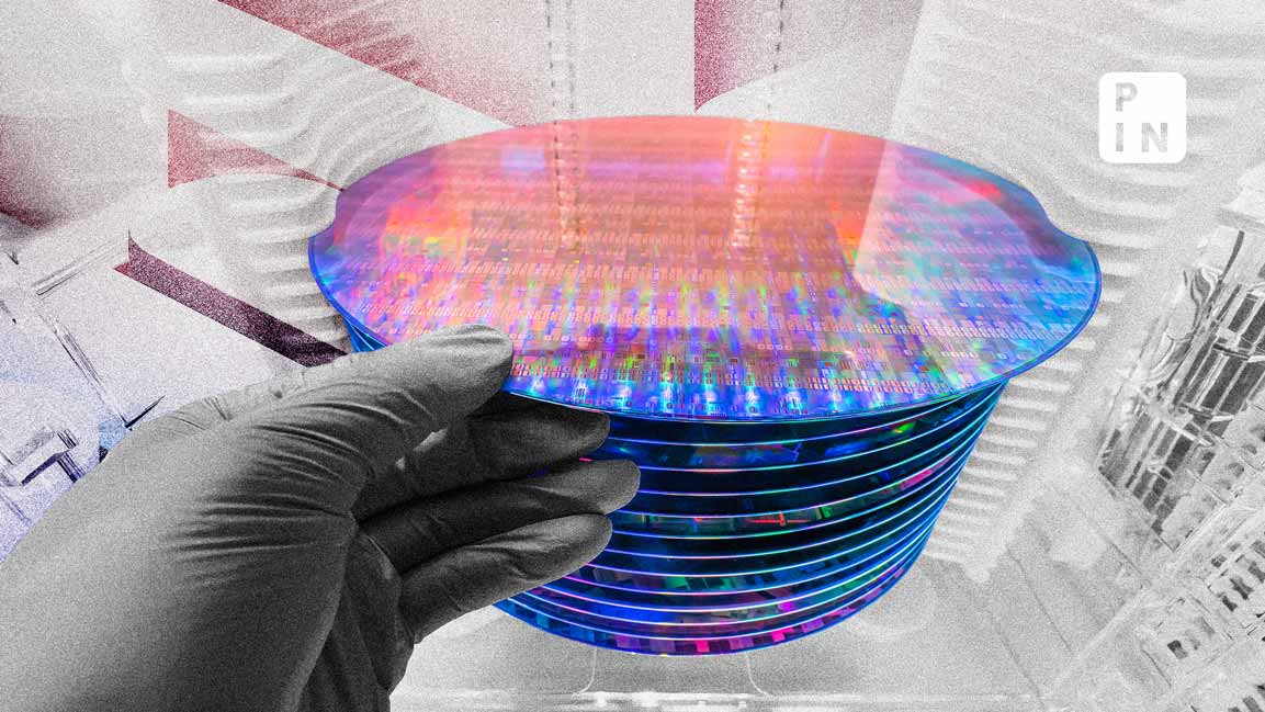


India has approved four new semiconductor projects worth ₹4,594 crore ($525 million) under the India Semiconductor Mission, reinforcing a push to expand domestic chipmaking capacity and cut reliance on imports.
Two plants will be set up in Odisha, with one each in Andhra Pradesh and Punjab, taking the number of sanctioned facilities to ten across six states.
The latest approvals bring projected investments under the program to about ₹1.6 trillion and are expected to generate more than 2,000 skilled jobs. They follow six other plants in Gujarat, Assam and Uttar Pradesh that have begun construction in the past six months.
Union electronics and IT minister Ashwini Vaishnaw said the government’s focus on streamlined clearances and compressed build timelines should see the new plants reach production within two to three years.
He linked the semiconductor drive to the Prime Minister’s aim of making technology accessible to all, noting that the India AI Mission has already made a 34,000-GPU computing facility available to innovators nationwide.
“The complete ecosystem of design, wafer fabrication, packaging, component manufacturing, assembly, testing, and high-volume final production is in the works,” he said. “Without semiconductors, no country can call itself developed.”
In Odisha, SiCSem Pvt. Ltd, working with Scotland’s Clas-SiC Wafer Fab, will build India’s first commercial silicon-carbide fabrication plant in Bhubaneswar.
The ₹2,066 crore unit will have an annual capacity of 60,000 wafers and 96 million packaged chips used in applications from space systems and missiles to satellites and rockets.
Also in the state, Heterogeneous Integrated Packaging Solutions Pvt. Ltd, a subsidiary of US-based 3D Glass Solutions, will invest ₹1,943 crore in an advanced packaging and embedded glass substrate facility, backed by equity from Intel, Lockheed Martin and Applied Materials.
It will be the first commercial-scale plant globally to offer 3D packaging on a glass substrate, with planned annual output of 70,000 glass panel substrates, 50 million assembled units and 13,200 3D integration modules.
In Punjab, Continental Device India Pvt. Ltd will expand its Mohali operations with a ₹117 crore investment to boost production of high-power discrete semiconductors such as MOSFETs, IGBTs and silicon carbide chips, raising annual output above 760 million units.
Andhra Pradesh will see Advanced System in Package Technologies, partnering with South Korea’s APACT, set up a ₹468 crore facility producing 96 million advanced packaging units a year for mobile devices, automobiles, set-top boxes and other electronics.
Vaishnaw said the projects would strengthen India’s position across the chip value chain—from design and wafer fabrication to packaging, assembly and high-volume production—with applications in defense, railways, data centers, consumer appliances and solar inverters.
The Cabinet’s decision builds on earlier big-ticket investments under the ISM, including Tata Electronics’ ₹91,000 crore fab in Gujarat and Micron Technology’s ₹23,000 crore packaging facility.
More Top Stories: